Semiconductor Device Engineering Methodology
First, through close exchanges with customers, UMS focuses on the comprehension of the targeted device: its specification, environment and application, and the associated technical challenges.
Then, UMS identifies the best approach for semiconductor processing, which is the best compromise between semiconductor manufacturability (ideal III-V technology versus performance targets, publication and patent verification,…) and cost-effectiveness.
Once this done, the process integration is defined to meet the product and application requirements.
- Process flow design
- Process module development
- Design of experiment
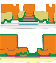
- Physical analysis (defect, process, device, …)
- Layout design or co-design with customers
- Risk assessment and definition of control plan
Finally, all technical and industrial aspects of the project management and execution are layed out.
- Project planning
- Project execution
- Project cost assessment and monitoring