
CHA3512-99F - 6-18GHz Low Noise DVA
Gain (dB)
16
Sat. Output Power (dBm)
23
Bias (mA)
210
Bias (V)
4.5
Dynamic Range (dB)
20
Noise Figure (dB)
7
P-1dB OUT (dBm)
20
RF Bandwidth (GHz) Max
18
RF Bandwidth (GHz) Min
6
Market
6-18GHz Chipset
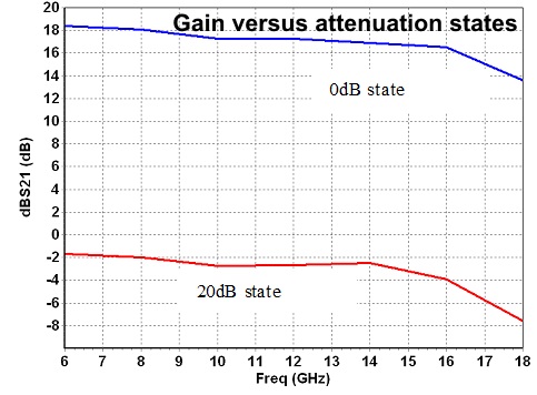
The CHA3512-99F is composed by a Single Pole Double Through (SPDT) switch followed by a one step digital attenuator and a double stage travelling wave amplifier.
It is designed for defense applications. The backside of the chip is both RF and DC grounded. This helps to simplify the assembly process.
The circuit is manufactured with a pHEMT process, 0.25µm gate length, via holes through the substrate, air bridges and electron beam gate lithography.
It is available in chip form.
Our latest Products
Get a glimpse of our latest product releases.


