Technologies – Front-End

GaAs MESFET (Metal-Semiconductor Field-Effect Transistor)

Basic Operation: GaAs MESFETs employ a Schottky barrier gate to modulate the channel conductivity in the GaAs substrate.  This traditional FET technology offers good high-frequency performance and relatively simple fabrication.

Key Features: Robust operation, moderate gain and frequency capabilities, good power handling, and linear operation.

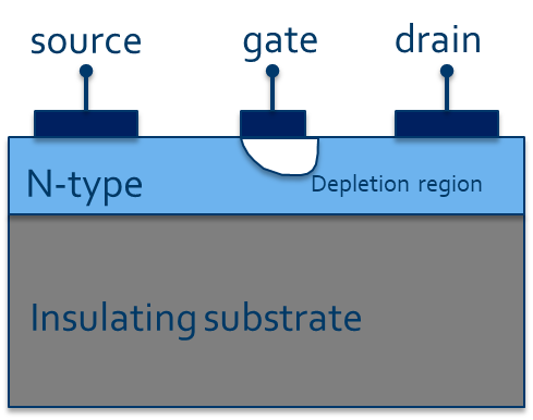
Figure: a cartoon of a MESFET structure. 

The basic principle of operation is as follows.  When there is a potential difference between source and drain terminals, the voltage on the gate modulates the current between them by means of a depletion region.  The active layer where this current forms is the n- doped region (shown in blue) and is constrained by the isolating substrate below.

The MESFET was first developed and demonstrated in research during the late 1960s and early 1970s. It began to be commercialized in the mid to late 1970s, particularly for microwave and RF applications due to its high-speed performance compared to silicon devices available at the time.  By early 1980s, MESFET technology had become established in commercial products, which offered superior electron mobility and frequency response than available Si technologies at that time.  MESFETs were widely adopted for low-noise amplifiers, microwave switches, and power amplifiers in radar, satellite, and early cellular communications.

Today this technology retains some advantages over successor technologies, and is used for specific applications such as analogue attenuators. 

HEMT (High Electron Mobility Transistor)

Basic Operation: A HEMT technology utilizes a heterojunction formed between different III-V semiconductor layers to create a two-dimensional electron gas (2DEG) with extremely high electron mobility.  This results in transistors with fast switching speeds and low noise figures, ideal for low-noise amplifiers and high-frequency active devices.

Key Features: High gain, low noise, high linearity, and high-frequency performance up to millimeter waves.

Figure: a cartoon of a HEMT structure. 

The basic principle of operation of a HEMT is similar to the MESFET, with current flowing between source and drain modulated by the gate voltage.  The structure differs in that several different III-V alloy materials are combined together exploiting their unique electrical characteristics to form a conductive region within the channel, commonly referred to as a two-dimensional gas, or 2DEG.  In the cartoon, the 2DEG is indicated as a dotted line.  An epitaxial process joins the different materials into a complex vertical structure engineering the electronic structure with atomic level precision.

For the GaAs system, the pseudomorphic HEMT or pHEMT was developed in the 1980s as a successor to the MESFET significantly improving frequency response and noise performance.  Within the heritage of UMS, Daniel Delagebeaudeuf and Tranc Linh Nuyen were among the pioneers of this device then working at Thomson-CSF (US patent 4,455,564).  pHEMT devices became commercially available by the early 1990s rapidly becoming a key component in modern high-frequency electronic devices.   Today, this technology is mainstream.  Several generations have been developed by UMS for use within its products and is also offered for foundry services.  

For the Gallium Nitride (GaN) system, HEMTs were developed starting in the early 1990s as researchers sought wide-bandgap semiconductor devices capable of handling high power and frequency; key milestones include the demonstration of high electron mobility channels on GaN/AlGaN heterostructures in the mid-1990s, the first commercial high-power GaN HEMT amplifiers emerging in the 2000s, and their widespread adoption in RF power amplifiers and power electronics for applications like radar, satellite communications, and 5G wireless networks.  For UMS, the first generation of GaN HEMT technology was released in 2012.   Since, there have been significant advancements in power density and power efficiency, and these technologies are for use in current UMS products and are also offered for foundry services.

HBT (Heterojunction Bipolar Transistor)

Basic Operation: The InP HBT technology leverages heterojunctions between different semiconductor materials to improve transistor speed and gain, enabling ultrafast switching and very high-frequency operation.

Key Features: Very high cutoff frequency (ft), low noise, and high gain.

Figure: a cartoon of a HBT structure.  Unlike the HEMT and MESFET, the current flow is vertical controlled by current rather than voltage.

The principle of operation is different than the aforementioned devices.  A III-V based HBT is a semiconductor device that uses different III-V materials joined together to form two heterojunctions.  The difference in the materials electronic properties is exploited to promote fast switching of large currents.  A HBT is a current-controlled device, meaning a base current modulates and amplifies the current captured by the collector.

The journey to the HBT begins with the invention of the Bipolar Junction Transistor (BJT) by Bell Labs in 1947, which was the first practical transistor and revolutionized electronics.  Subsequently, the combination of different III-V alloys and the formation of heterojunctions improved frequency response and achieved exponentially more current flow.  The maturation of epitaxial manufacturing processes have propelled HBTs to wide adoption.  UMS manufactures GaAs based HBT technologies, which primarily serve applications that require modest RF power and/or challenging linearity specifications.